
Contact Us
Don't Let Your Chips Fry: The Engineer's Guide to Thermal Conductive Silicone Pads
Last week, my high-end gaming laptop started stuttering mid-raid. Fans roared at max speed, but the frame was hot enough to cook eggs. I pulled off the cooler—and there it was. The factory thermal pad had turned into a crumbly, dried-out mess. That little grey sheet was the only thing standing between my GPU and a thermal shutdown.
That’s when I realized: thermal pads are boring, until they fail. Then they become the most important component in your system.
If you design, build, or repair electronics, you need to understand thermal conductive silicone pads. Not just what they are, but how to choose, apply, and source them without burning time and money. Let’s dive in.
What Is a Thermal Conductive Silicone Pad? (And Why Should You Care?)
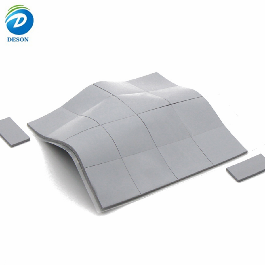
A thermal conductive silicone pad is a soft, compliant sheet that sits between a heat source (like a CPU, power transistor, or LED array) and a heat sink or chassis. Its job is simple: push heat out of the hot part and into the cooling hardware.
But the magic is in the gaps. No two surfaces are perfectly flat. Microscopic air gaps act like thermal blankets—trapping heat. A silicone pad squishes into those gaps, replacing air (a terrible conductor) with a engineered material that moves heat efficiently.
Think of it as a thermal bridge. Without it, your chip might as well be screaming into a pillow.
How Do These Pads Actually Work?
They don’t pump heat or blow air. Instead, they rely on conductive fillers suspended in a silicone polymer matrix. The silicone provides softness and conformity; the fillers (usually ceramic or mineral particles) create heat-conduction highways.
When compressed between two surfaces, the pad:
Deforms to fill microscopic valleys and peaks.
Transfers vibrational energy from hot molecules to cooler ones.
Spreads heat from a small hotspot to a larger heat sink area.
You’ll find them in IC packages, COF (chip-on-flex) displays, EV battery modules, LED luminaires, wireless chargers, and pretty much any sealed electronics enclosure.
Common Materials at a Glance (Table + Advantages)
Not all thermal pads are created equal. Here’s a quick cheat sheet on the most popular material families—and when to use each.
| Material Type | Key Advantages | Typical Thermal Conductivity (W/m·K) | Best For |
| Standard Silicone Pad (alumina/BN filled) | Soft, conformable, electrically insulating, easy to cut | 1.0 – 6.0 | General purpose CPU/GPU, power supplies, LED |
| Fiberglass-reinforced Silicone | Tear-resistant, dimensional stable, good for automated assembly | 1.5 – 3.0 | High-vibration environments, automotive, handheld devices |
| Graphite Sheet | Extremely high in-plane conductivity (up to 1500+ W/m·K through-plane lower) | 10 – 30 (in-plane) | Thin laptops, smartphones, where lateral heat spreading is critical |
| Silicone Foam Pad | High compressibility, vibration damping, gap-filling for uneven gaps | 1.0 – 2.5 | Battery packs, large uneven castings, outdoor enclosures |
| Phase Change Material (PCM) on silicone carrier | Melts at operating temp for near-zero interface resistance, but re-solidifies | 3.0 – 8.0 | High-performance CPUs, GPUs, IGBT modules (better than paste in some automated lines) |
| Ceramic-filled Polyimide | Ultra-thin, high dielectric strength, no silicone outgassing | 1.0 – 2.0 | Aerospace, optical sensors, cleanroom environments |
Pro tip: Don’t chase the highest W/m·K number. A stiff, high-conductivity pad that doesn’t conform to your surface will perform worse than a softer, lower-conductivity pad that wets out perfectly.
The Manufacturing Reality Check (What Datasheets Don’t Tell You)
Engineers often pick a pad based on thermal specs alone. Then production calls, furious. Why? Because making thermal pads into finished parts is trickier than it looks.
1. Material Form: Roll vs. Sheet
Most thermal silicone comes in rolls (continuous length) or sheets (e.g., 300x300mm). Rolls are cheaper per area but require slitting and converting. Sheets are easier for manual placement but waste more material.
Hidden cost: Small rolls mean frequent roll changes on a die-cutter. Each change eats 10–20 minutes of machine time and creates scrap. For a run of 500 pads, that can double your piece price.
2. Thickness – The Goldilocks Problem
Too thin, and the pad won’t touch both surfaces. Too thick, and it over-compresses, potentially warping boards or cracking solder joints. Also, stacking two thin pads instead of one thick one is a bad idea—every interface adds thermal resistance and increases assembly error.
Rule of thumb: Target 15–30% compression. If your gap varies by 0.5mm, choose a pad that can accommodate that range without bottoming out.
3. Soft & Sticky Materials Need Backing
Very soft pads (Shore 00 < 40) are great for low-pressure gaps, but they stretch, tear, and stick to everything. To die-cut them cleanly, you need a structural carrier liner (like PET) that gets peeled off after application. That adds cost and handling steps.
4. Quantity – The Customization Trap
Most thermal pad jobs are low volume (hundreds of pieces) and highly customized. Material is expensive. Tooling (die, kiss-cut fixtures) amortized over 500 parts can be brutal. That’s why many engineers end up hand-cutting with an X-Acto knife—which works for prototypes, but not for 500 units.
What to do: For simple square or rectangular pads without adhesive, buy precut sheets online. For complex shapes (holes, notches, pull tabs, stepped thicknesses), find a converter (a die-cutting specialist) early in your design phase.
The Bottom Line
Thermal conductive silicone pads aren’t glamorous. But when your product runs cool, stays reliable, and doesn’t melt down in the field, that boring grey pad just saved your reputation.
Don’t let your chips fry. Choose wisely, prototype early, and work with people who understand both the thermodynamics and the manufacturing floor.
Have a tricky gap or a weird shape? Reach out to a reputable converter (I’m happy to point you to a few – just drop a comment below). And if you want to dive deeper, download our free thermal interface material selection matrix – link in bio.
Stay cool, engineers.